TSMC Reaches 2nm Milestone
TSMC has made a major breakthrough in advanced semiconductor manufacturing with its 2nm technology. The company achieved a reported 60% yield in a recent trial production run, bringing it closer to full-scale volume production. According to details shared at IEDM 2024, TSMC’s N2 technology promises a 30% power improvement and 15% performance gain over the precious 3nm node. Optimized for AI, mobile and HPC applications, this technology delivers significant advantages for chip designers, including increased performance, higher density, reduced power consumption and advanced power management capabilities.
A Closer Look at TSMC’s N2 Technology & NanoFlex Innovation

The industry is pushing towards smaller, more efficient nodes. TSMC aims to lead the way with its advanced N2 technology, which it claims will set new standards in both density and energy efficiency. The company plans to secure its technology leadership by making continuous enhancements to N2 and its derivatives.
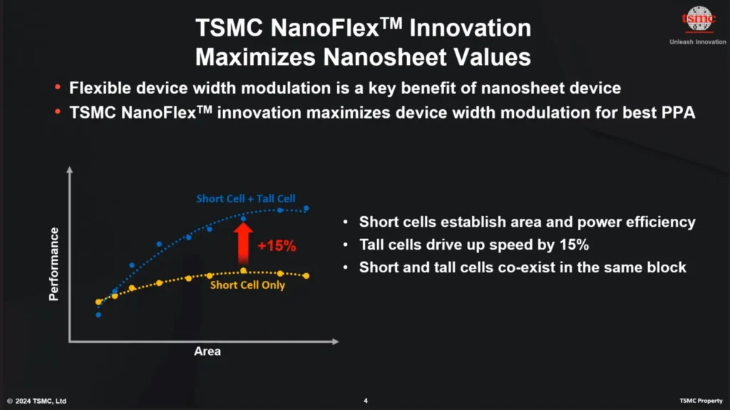
TSMC’s NanoFlex Technology introduces a new level of design flexibility, allowing engineers to optimize for specific performance and efficiency goals.
Key benefits include:
- Higher performance through advanced transistor designs
- Greater density to accommodate more transistors per chip
- Enhanced power management to reduce energy consumption
With NanoFlex, designers can mix and match standard cells from different libraries within the same block, unlocking new possibilities for customized chip optimization.
Production Updates, Expected Costs & Industry Adoption
Following promising early yield reports, it is expected that TSMC will begin full-scale volume production by 2026. The shift to 2nm comes at a steep cost however, with industry experts estimating that 2nm wafers could be as high as $30,000, nearly twice the price of 4nm and 5nm wafers. This surge will impact market segmentation, likely limiting early adoption to high-margin applications like HPC, advanced AI accelerators and premium mobile devices. Major companies like Apple and NVIDIA are expected to adopt TSMC’s N2 node for their next-generation products. According to analyst Ming-Chi Kuo, Apple’s 2026 iPhone lineup may feature 2nm chips, but likely only in Pro models due to cost constraints.
What’s next for TSMC’S 2nm Technology?
Looking ahead, TSMC’s 2nm technology will play a pivotal role in shaping future innovations in high-performance computing, artificial intelligence and beyond. As the company moves closer towards volume production, the 2nm node will continue to evolve, with further improvements to yield, cost-effectiveness and design flexibility. TSMC’s focus on innovation through NanoFlex technology will enable chip designers to create highly customized solutions, further enhancing the capabilities of next-generation devices. While the higher costs associated with 2nm wafers may limit initial adoption, TSMC’s partnerships with leading tech companies, such as Apple and NVIDIA, will likely accelerate the industry’s adoption of this new technology.

